


India's semiconductor strategy entered a more demanding phase in 2026. The country is no longer discussing chips only through future factories and incentive approvals. Micron's ATMP facility, Kaynes Semicon and CG Semi have started commercial production, according to the government. At the same time, the Union Cabinet has approved Semicon 2.0 with a total outlay of ₹1,27,500 crore.
These milestones are important, but they do not mean India already has a self-sufficient chip industry. Packaging output is different from wafer fabrication, and an approved plant is different from a facility operating at qualified yields. The investment case now rests on execution across design, fabrication, packaging, materials, utilities and customer qualification.
This article uses the supplied Equirus report and current government releases to assess where India has made measurable progress, where dependence remains high and what evidence matters next.
Why does India want a domestic semiconductor industry?
Semiconductors sit inside smartphones, vehicles, telecom networks, industrial machinery, medical devices, defence systems and data centres. Disruption at a small number of overseas fabrication or packaging hubs can therefore affect production across several Indian industries. The chip shortage that followed the pandemic made this concentration visible.
Domestic demand strengthens the strategic argument. Electronics manufacturing, vehicle electrification, 5G deployment and data-centre construction all increase chip content. The supplied Equirus report estimates India's semiconductor consumption at US$62 billion in 2026 and US$155 billion by 2031. These are research estimates rather than official procurement commitments, but they illustrate the size of the potential market.
India also begins with an established design base. Global semiconductor companies operate large engineering centres in the country, while government programmes are extending electronic-design-automation tools to startups and academic institutions. This gives India a stronger starting point in architecture and verification than many late entrants had.
The strategic objective should not be interpreted as eliminating all imports. No major semiconductor economy controls every tool, material and technology node. A more realistic goal is to build reliable domestic capacity in selected layers while becoming a trusted participant in global supply chains.
See what markets are pricing in
Live indices, sector moves and market breadth — the backdrop to every story we publish.
What progress has India made by 2026?
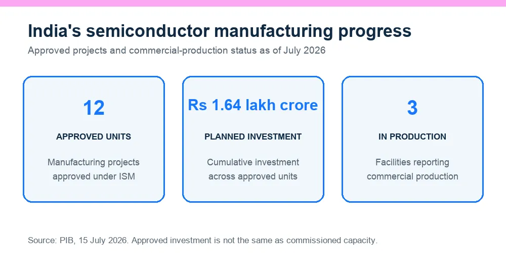
The July 2026 Semicon 2.0 announcement says 12 manufacturing units have been approved with cumulative planned investment above ₹1.64 lakh crore. The portfolio includes one silicon fab, one silicon-carbide fab, an integrated gallium-nitride micro-LED display fab and nine packaging units. Three facilities had started commercial production.
This marks a transition from policy intent to physical output, especially in assembly, testing, marking and packaging. Micron's Sanand facility began commercial production and shipment of memory modules in February 2026. Kaynes Semicon's Sanand plant was inaugurated in March. CG Semi also entered commercial production, according to the July Cabinet release.
Packaging is a sensible entry point. It usually requires less capital and process complexity than an advanced logic fab, while creating experience in cleanroom operations, quality control, testing and customer qualification. It can serve automotive, industrial, power-electronics and consumer applications that use mature technologies.
The Tata-PSMC fab at Dholera is the larger test of fabrication capability. Government approvals describe planned capacity of about 50,000 wafer starts per month. The supplied report expects initial chip output around the end of 2026, but commissioning schedules can move. Construction completion, tool installation, process transfer and customer qualification should be tracked separately.
Approved investment is therefore a pipeline measure. It should not be treated as commissioned capacity, revenue or import substitution. The next phase must demonstrate repeatable volumes and competitive economics.
How does the semiconductor value chain create value?
A chip moves through several specialised layers. Designers define its architecture and functionality using intellectual property and EDA software. A foundry fabricates circuits on wafers through hundreds of tightly controlled process steps. Packaging companies cut, assemble, connect and test the dies before electronics manufacturers place them in finished systems.
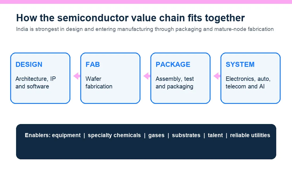
The economics vary sharply. Design and software can earn high margins because differentiated intellectual property scales without a new factory for every unit. Fabrication is capital-intensive and depends on yield, utilisation and frequent technology investment. Packaging generally has lower margins, but offers a more accessible manufacturing entry point.
India's opportunity is not limited to headline fabs. Semiconductor plants consume specialty chemicals, industrial gases, substrates, precision components, cleanroom systems, water-treatment equipment and uninterrupted power. The supplied report estimates import dependence above 90% for many semiconductor inputs. That number is a report estimate, but the direction is clear: factories alone do not create a complete ecosystem.
| Value-chain layer | India's current advantage | Main execution gap |
|---|---|---|
| Chip design | Large engineering base and global capability centres | More domestic product IP and commercial scale |
| Wafer fabrication | Policy support and first major fab under development | Process transfer, yields, utilities and customers |
| OSAT/ATMP | Multiple approved units and commercial production | Utilisation, qualification and margin discipline |
| Equipment and materials | Existing engineering and chemical suppliers | Semiconductor-grade purity and qualification |
| End-market demand | Large electronics, auto, telecom and data-centre markets | Greater domestic component value addition |
What does Semicon 2.0 change for the industry?
Semicon 1.0 established fiscal support for fabrication, compound semiconductors, packaging and design. The original programme had an outlay of ₹76,000 crore and offered support of up to 50% for eligible manufacturing projects. State incentives could add land, power and capital support.
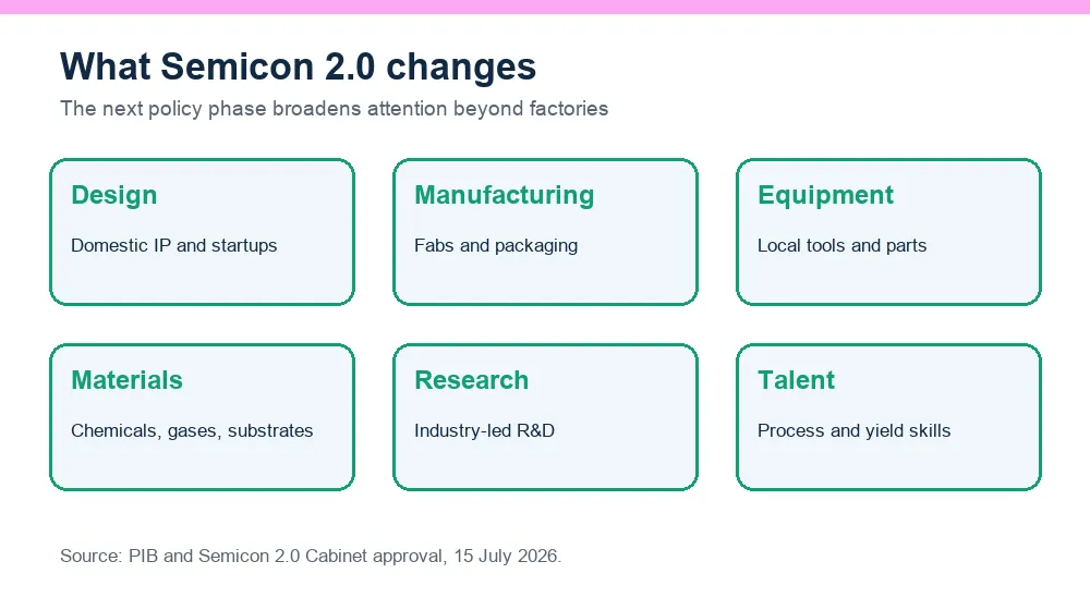
Semicon 2.0 broadens the policy focus. The Cabinet approval announced in July 2026 carries an outlay of ₹1,27,500 crore and describes six pillars, including design, manufacturing, equipment, materials, research and talent. This is a useful shift because the hardest gaps increasingly sit around factories rather than only inside them.
The design side also shows early activity. The government reported 24 semiconductor design projects approved for financial support and 105 startups or MSMEs with access to EDA tools. These companies still need prototypes, qualified products, customer wins and recurring revenue before programme participation becomes commercial success.
Policy support can absorb part of the capital burden, but it cannot guarantee yields, utilisation or technology relevance. Incentives should be evaluated alongside private capital committed, project milestones achieved and the durability of the underlying demand.
Get research like this in your inbox
The week’s research that mattered, in five minutes. Joined by 2L+ investors.
Where can Indian semiconductor companies create durable value?
The most durable value may emerge where local capabilities solve a specific customer problem. In design, that could mean power-management chips, motor controllers, communications components, defence electronics or industrial devices with identifiable domestic demand. Fabless companies can scale with less capital than manufacturers, although design cycles are long and customer qualification is demanding.
Packaging companies can benefit as local and global customers seek geographically diverse capacity. Their returns will depend on utilisation, package complexity, yields and pricing rather than installed capacity alone. Advanced packaging can create more value than basic assembly, but it requires deeper process control and closer customer relationships.
Equipment and material suppliers offer another path. An Indian company that qualifies a high-purity chemical, gas system, cleanroom component or testing product can sell across several projects. Qualification creates barriers to entry, but the standards are exacting and failure costs are high.
Electronics manufacturers may also gain from shorter supply chains and collaborative product development. However, local packaging does not automatically mean the underlying die was designed or fabricated in India. Investors should distinguish domestic value addition from a product's final country-of-origin label.
What risks could slow India's semiconductor ambitions?
Execution is the immediate risk. Semiconductor projects are complex, and schedule delays can increase costs before revenue starts. Once a facility opens, low utilisation can damage returns because depreciation, skilled labour and utility expenses continue.
Yield is equally important. A plant can produce wafers or packaged units without producing enough saleable output. Customer qualification can take months, especially for automotive, industrial and strategic applications where reliability requirements are strict.
Infrastructure has to be consistent, not merely available. Fabs need stable power, large volumes of ultra-pure water, controlled logistics and rapid equipment service. Packaging plants need reliable substrates, materials and testing capability. A weakness in one input can interrupt the entire line.
Technology selection creates another risk. India is targeting mature nodes and specialised products that serve large real-world markets. That is rational, but each plant still needs customers whose products remain competitive over the asset's life. Capacity built without committed demand can become expensive idle infrastructure.
Finally, geopolitical diversification is an opportunity and a constraint. India may win projects as customers seek alternatives, but critical tools, intellectual property and materials remain concentrated among a few countries and companies. Export controls or trade disputes can still affect schedules.
How should investors assess India's semiconductor opportunity?
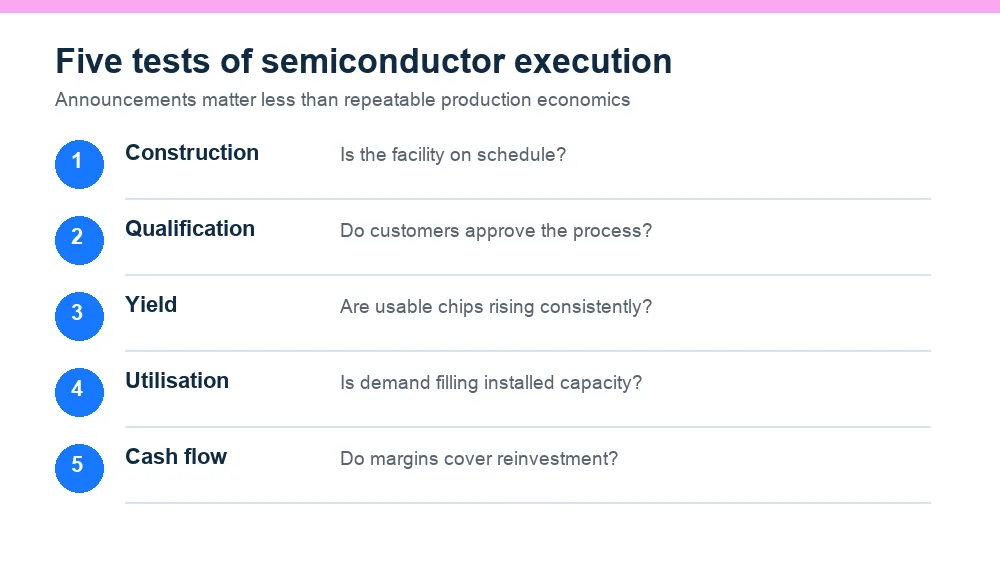
Investors should separate national ambition from company economics. A growing domestic chip market does not guarantee that every project will earn attractive returns. Order announcements should be reconciled with facility readiness, customer qualification, capital spending and cash collection.
Useful operating evidence includes commercial shipments, production yields, utilisation, repeat orders and the share of revenue earned from qualified higher-value products. For suppliers, investors should examine semiconductor-grade certification and customer concentration. For fabless companies, tape-outs matter, but customer adoption and recurring product revenue matter more.
Balance-sheet exposure deserves attention because fabrication and packaging require capital before volumes mature. Subsidy receivables, project debt, cost overruns and continuing technology investment can change returns materially. Comparisons should also account for whether a company owns the plant, supplies equipment, integrates packages or licenses intellectual property.
India has crossed an important threshold in 2026: commercial semiconductor production is now real. Building a complete ecosystem will take longer. The strongest evidence will come from qualified products, improving yields, local supplier development and cash flows that persist after incentives.
Follow this sector’s live moves
Sector-level performance across Indian markets, updated through the day.
What are the key FAQs about India's semiconductor industry?
Does India manufacture semiconductor chips in 2026?
Yes. Commercial production has begun at packaging and testing facilities including Micron, Kaynes Semicon and CG Semi. Large-scale domestic silicon wafer fabrication remains under development.
How many semiconductor projects has India approved?
As of July 2026, the government reported 12 approved semiconductor manufacturing units with cumulative planned investment above ₹1.64 lakh crore.
What is the difference between a fab and an OSAT facility?
A fab creates circuits on silicon wafers. An OSAT facility assembles, packages and tests fabricated dies before they are used in electronic products.
What is Semicon 2.0?
Semicon 2.0 is India's expanded semiconductor programme covering design, manufacturing, equipment, materials, research and talent, with an announced outlay of ₹1,27,500 crore.
What should determine the success of India's chip strategy?
Success should be judged through qualified commercial products, yields, utilisation, domestic supplier depth, customer adoption and sustainable cash flow, not project approvals alone.